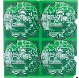
Rf pcb guidelines
Best Practices For Rf pcb guidelines
Designing a printed circuit board (PCB) for radio frequency (RF) applications requires meticulous attention to detail and adherence to best practices to ensure optimal performance.
The complexity of RF signals, which can be highly susceptible to interference and signal degradation, necessitates a strategic approach to PCB layout.
By following established guidelines, designers can mitigate potential issues and enhance the functionality of their RF circuits.
To begin with, one of the most critical aspects of RF PCB design is the careful management of signal integrity.
This involves maintaining consistent impedance throughout the signal paths, which can be achieved by using controlled impedance traces. These traces should be designed with precise width and spacing, taking into account the dielectric properties of the PCB material. Additionally, it is essential to minimize the length of high-frequency signal paths to reduce the risk of signal loss and reflection.
Another key consideration is the placement of components.
RF components should be strategically positioned to minimize the length of interconnecting traces and to avoid unnecessary bends, which can introduce inductance and capacitance. Placing sensitive components, such as low-noise amplifiers and mixers, away from high-power circuits can help reduce electromagnetic interference (EMI). Furthermore, grounding is paramount in RF PCB design. A solid ground plane can provide a low-impedance return path for signals, thereby reducing noise and improving overall signal integrity.
Transitioning to the topic of power supply design, it is crucial to ensure that the power supply is clean and stable.
Power supply noise can significantly impact the performance of RF circuits. To mitigate this, designers should use decoupling capacitors close to the power pins of active components. These capacitors can filter out high-frequency noise and provide a stable voltage supply. Additionally, using low-dropout regulators (LDOs) can help maintain a consistent voltage level, further enhancing the performance of the RF circuit.
Thermal management is another important aspect that cannot be overlooked.
RF components can generate significant amounts of heat, which, if not properly managed, can lead to performance degradation or even failure. Effective thermal management strategies include the use of thermal vias, heat sinks, and proper PCB layout techniques to dissipate heat away from critical components. Ensuring adequate airflow around the PCB can also help maintain optimal operating temperatures.
Moreover, shielding is a vital practice in RF PCB design to protect sensitive circuits from external EMI and to prevent the RF signals from radiating and causing interference with other systems.
Shielding can be implemented using metal enclosures or by incorporating ground planes and guard traces around critical signal paths. This practice not only enhances the performance of the RF circuit but also ensures compliance with regulatory standards for electromagnetic compatibility (EMC).
In conclusion, designing an RF PCB requires a comprehensive understanding of various factors that influence signal integrity, component placement, power supply stability, thermal management, and shielding. By adhering to these best practices, designers can create robust and reliable RF circuits that perform optimally in their intended applications. The meticulous attention to detail and strategic planning involved in RF PCB design ultimately contribute to the successful deployment of high-performance RF systems.
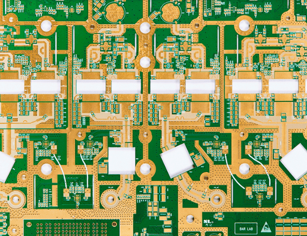
Material Selection For RF PCB Applications
When designing RF PCBs, the selection of materials is a critical factor that significantly influences the performance, reliability, and manufacturability of the final product. The choice of substrate material, in particular, plays a pivotal role in determining the electrical properties, thermal management, and mechanical stability of the RF circuit. Therefore, understanding the key considerations for material selection is essential for engineers and designers working in RF applications.
To begin with, the dielectric constant (Dk) of the substrate material is a primary consideration.
The dielectric constant affects the signal propagation speed and impedance of the transmission lines. Materials with a low and stable dielectric constant are preferred for high-frequency applications because they minimize signal loss and ensure consistent performance across a wide frequency range. Common materials used in RF PCBs include PTFE (Polytetrafluoroethylene), ceramic-filled PTFE composites, and high-frequency laminates such as Rogers materials. These materials offer low dielectric constants and low loss tangents, making them suitable for high-speed and high-frequency circuits.
In addition to the dielectric constant, the thermal properties of the substrate material are equally important.
RF circuits often generate significant amounts of heat, and efficient thermal management is crucial to maintain performance and prevent damage. Materials with high thermal conductivity help dissipate heat more effectively, ensuring the longevity and reliability of the PCB. For instance, ceramic-filled PTFE composites not only provide excellent electrical properties but also offer superior thermal conductivity compared to standard FR-4 materials.
Moreover, the coefficient of thermal expansion (CTE) is another critical factor to consider.
The CTE measures how much a material expands or contracts with temperature changes. A substrate material with a CTE that closely matches that of copper is ideal, as it minimizes the risk of delamination and mechanical stress during thermal cycling. This is particularly important in RF applications where temperature variations are common. Materials like PTFE and certain high-frequency laminates exhibit low CTE values, making them suitable choices for RF PCB applications.
Furthermore, the mechanical properties of the substrate material should not be overlooked.
The material must provide sufficient rigidity and durability to withstand the mechanical stresses encountered during manufacturing, assembly, and operation. Flexibility and toughness are also important considerations, especially for applications involving flexible or rigid-flex PCBs. High-frequency laminates and PTFE composites generally offer good mechanical stability, ensuring the structural integrity of the RF PCB.
Additionally, the manufacturability of the chosen material is a practical consideration.
Some high-performance materials may require specialized processing techniques, which can increase production complexity and cost. Therefore, it is essential to balance performance requirements with manufacturability to achieve an optimal design. Collaborating with PCB manufacturers early in the design process can help identify materials that meet both performance and production criteria.
Lastly, environmental factors such as moisture absorption and chemical resistance should be taken into account.
Materials that absorb moisture can experience changes in dielectric properties, leading to signal degradation. Therefore, selecting materials with low moisture absorption rates is crucial for maintaining consistent performance in varying environmental conditions. Similarly, chemical resistance ensures that the material can withstand exposure to harsh chemicals during manufacturing and operation without degrading.
In conclusion, the selection of materials for RF PCB applications involves a careful evaluation of electrical, thermal, mechanical, and environmental properties. By considering factors such as dielectric constant, thermal conductivity, CTE, mechanical stability, manufacturability, and environmental resistance, designers can make informed decisions that enhance the performance and reliability of RF circuits. Through meticulous material selection, the challenges associated with high-frequency PCB design can be effectively addressed, leading to successful and robust RF applications.
Techniques For Minimizing Signal Loss In RF PCBs
When designing RF PCBs, minimizing signal loss is paramount to ensure optimal performance and reliability. Signal loss in RF circuits can lead to degraded performance, reduced range, and increased power consumption. Therefore, employing effective techniques to mitigate these losses is essential.
One of the primary considerations is the choice of materials.
High-frequency laminates, such as Rogers or Taconic, are preferred over standard FR4 due to their lower dielectric constant and loss tangent. These materials help maintain signal integrity by reducing dielectric losses, which are a significant contributor to signal attenuation.
Another critical factor is the design of the transmission lines.
Microstrip and stripline configurations are commonly used in RF PCB designs. Microstrip lines, which consist of a conductive trace on a dielectric substrate with a ground plane on the opposite side, are simpler to fabricate but can suffer from higher radiation losses. Striplines, on the other hand, are sandwiched between two ground planes, providing better shielding and reduced radiation losses. However, they are more complex to manufacture. The choice between microstrip and stripline depends on the specific application requirements and trade-offs between ease of fabrication and performance.
Impedance matching is another crucial aspect of minimizing signal loss.
Mismatched impedance can cause reflections, leading to signal degradation and power loss. To achieve proper impedance matching, careful calculation and design of the transmission line width, spacing, and dielectric thickness are necessary. Tools such as impedance calculators and simulation software can aid in this process, ensuring that the characteristic impedance of the transmission lines matches the source and load impedances.
In addition to impedance matching, minimizing signal loss also involves reducing parasitic effects.
Parasitic capacitance and inductance can introduce unwanted resonances and signal degradation. To mitigate these effects, it is essential to keep the traces as short and direct as possible. Avoiding sharp bends and using gradual curves can help reduce inductive effects. Additionally, placing ground vias close to the signal traces can minimize parasitic inductance and improve signal integrity.
Grounding and shielding play a vital role in minimizing signal loss in RF PCBs.
A solid ground plane provides a low-impedance return path for the signals, reducing ground loops and noise. Ensuring a continuous ground plane with minimal interruptions is crucial. In cases where a continuous ground plane is not feasible, stitching vias can be used to connect different ground planes, maintaining a low-impedance path. Shielding techniques, such as using metal enclosures or ground planes above and below the signal traces, can further reduce electromagnetic interference and signal loss.
Furthermore, the layout of components and traces should be carefully considered.
Placing sensitive components away from noisy ones and routing high-frequency signals away from low-frequency signals can minimize crosstalk and interference. Proper decoupling and bypass capacitors should be strategically placed to filter out noise and provide stable power to the RF components.
Finally, manufacturing tolerances and quality control are essential to ensure that the designed RF PCB performs as intended.
Variations in trace width, dielectric thickness, and material properties can impact the impedance and signal integrity. Therefore, working closely with the PCB manufacturer and specifying tight tolerances can help achieve consistent and reliable performance.
In conclusion, minimizing signal loss in RF PCBs requires a comprehensive approach that encompasses material selection, transmission line design, impedance matching, parasitic effect reduction, grounding, shielding, component layout, and manufacturing quality. By carefully considering these factors and employing best practices, designers can achieve high-performance RF circuits with minimal signal loss, ensuring reliable and efficient operation.
Importance Of Grounding And Shielding In RF PCB Design
In the realm of RF PCB design, the importance of grounding and shielding cannot be overstated. These two elements are fundamental to ensuring the optimal performance and reliability of RF circuits. Grounding and shielding serve as the bedrock upon which the integrity of RF signals is maintained, mitigating the adverse effects of electromagnetic interference (EMI) and ensuring signal fidelity.
To begin with, grounding in RF PCB design is crucial for establishing a common reference point for all electrical signals.
A well-designed ground plane minimizes the potential differences across the PCB, thereby reducing noise and crosstalk between different circuit components. This is particularly important in RF circuits, where even minor variations in potential can lead to significant signal degradation. By providing a low-impedance path to ground, the ground plane helps in stabilizing the circuit and enhancing its overall performance.
Moreover, the placement and layout of the ground plane are critical considerations.
It is essential to ensure that the ground plane is continuous and unbroken, as any discontinuities can create impedance mismatches and reflection points, which can severely impact signal integrity. Additionally, the ground plane should be as close as possible to the signal traces to minimize the loop area and reduce the inductive coupling of noise. This proximity helps in maintaining a low impedance path for the return currents, thereby reducing the potential for EMI.
Transitioning to the concept of shielding, it is equally vital in RF PCB design.
Shielding involves the use of conductive materials to enclose sensitive components and signal traces, thereby protecting them from external electromagnetic fields. This is particularly important in environments with high levels of EMI, where unshielded circuits can easily pick up unwanted noise, leading to signal distortion and degradation.
Effective shielding requires careful consideration of the materials and techniques used.
Conductive enclosures, such as metal cans or Faraday cages, are commonly employed to provide a physical barrier against EMI. Additionally, the use of ground planes and vias to create a shielded environment within the PCB itself can be highly effective. These techniques help in isolating sensitive components from external noise sources, thereby preserving the integrity of the RF signals.
Furthermore, the integration of grounding and shielding techniques can significantly enhance the overall performance of RF circuits.
For instance, the use of a ground plane in conjunction with shielding enclosures can create a highly effective barrier against EMI. This combination helps in maintaining a stable reference potential while simultaneously protecting sensitive components from external noise. Additionally, the use of decoupling capacitors and ferrite beads can further enhance the effectiveness of grounding and shielding by filtering out high-frequency noise and providing additional isolation.
In conclusion, grounding and shielding are indispensable elements in RF PCB design. They play a pivotal role in maintaining signal integrity, reducing noise, and ensuring the reliable operation of RF circuits. By carefully considering the layout and implementation of grounding and shielding techniques, designers can significantly enhance the performance and reliability of their RF designs. As the demand for high-frequency and high-performance RF circuits continues to grow, the importance of grounding and shielding will only become more pronounced, underscoring their critical role in the field of RF PCB design.